
Does Copper Block EMF? Understanding the Role of Copper in Mould Base Shielding Applications
Copper – you know, that reddish-orange metal that’s easy to work with and has all these nifty electrical conductivty traits? Yeh, people tend to associate it with electrical wiring or decorative elements. But lately — I dunno maybe through working on this project or just stumbling upon a new interest in electromagnetic fields — I found that some folks were wondering if copper could block EMF. But wait… does copper really block emf? Especially within more niche domains like mold bases (sometimes misspell as 'mould base', like myself before diving deep into manufacturing), things start getting even weirder.
(Side note: I’ve caught up recently in my research and have started messing around with different shielding materials; turns out, I'm fascinated by the intersection of traditional manufacturing practices & EM protection tech.) And what better place for such experimentation than the industrial use-cases where mold base design actually overlaps with electromag considerations – like precision components housed within sensitive molds. If your part needs RF shielding, grounding pathways or EMI containment during manufacturing? Then read on… and prepare yourself to question what copper can or can’t do.
Dose Check: Does Copper Actally ‘Block’ EMF Like We Hope?
Alright so the first question is – when you're designing a product that uses an EM field shield or dealing directly with a high-frequency process… can just slapping in a chunk of copper stop interference from spreading everywhere or absorbing it?
No one likes interference noise. That's not a debate. When building tools that interact with radio waves, wireless communication devices, power circuitry inside machines or industrial systems exposed to electromagnetic pollution? There must be proper shielding measures in place. But does copper live up to expectations, or am I just chasing myths?
- Magnetism-wise – nope. Doesn't stop magnetic flux unless you make thick plates and add multiple layers
- For electric fields - it definitely conducts well and creates what we sometimes refer to as ‘cages’ (faraday) that absorb unwanted charges
- In cases where frequency isn’t super ultra high (like 2MHz and under), solid copper panels do provide moderate but effective protection
- The higher end frequencies – you’ll often need specialized foils or composite layers alongside other metals
| EM Field Type | Copper Behavior | Recommended Use Case |
|---|---|---|
| Low-frequency | High conductivity = good ground path = helps contain charge buildups | Easily implemented grounding structures / PCB boards / cable connectors |
| Moderate freq. radiation | Absorbs partial energy – acts as basic RF blocker depending on skin thickness | Cabinets or housing for semi-sensitive devices – especially near transformers/motors |
| Ultra high freq (microwaves/6G+?) | Loses some blocking performance due surface skin effect limits at extreme ranges | Best in layered form, paired with aluminum/beryllium-copper alloys in critical defense gear or space hardware |
I had this assumption early on: “put copper plate over opening and voilà!" Nope. Not quite how real physics work.

Facts About Copper’s Real Limitations for Industrial EM Mitigation
If you're reading up on whether copper shields your machine’s sensitive electronics or stops stray currents running wild through nearby circuits—don’t believe every blog headline.
Here's where people get confused:
I saw countless Reddit users claiming copper blocks WiFi and stuff like that – and they’re mostly wrong because wifi's signal doesn't really get "stopped" so much as attenuated depending on orientation & coverage area. In short – sure, partially, if done very strategically with the right alloy composition. The key here being strategic deployment rather than blind assumptions about metal alone working as an ultimate solution.
"Conductivity alone won’t magically null EM energy... You also gotta manage permeability factors when working with high flux environments."
You don’t have perfect isolation using simple copper cladding. So if you've built a DIY box to keep microwave radiation from bleeding through walls, rethink that setup.
The Mold Base Mystery Explained Briefly
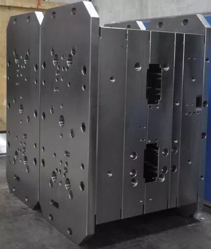
The next logical piece here is about how the whole EM shielding narrative collides (maybe awkwardly at times) with actual mechanical production parts like the famed 'mold base' – a foundational component for injection molding setups' used primarily in making complex plastic shapes at scale via heavy automated presses. So what's the relation? Well it turns out in high-speed production runs, where precision matters greatly – say aerospace micro components – there exists scenarios were stray induction spikes or electrostatic discharges inside your diecast chamber might disrupt processes. If you're integrating sensors within smart molding units, proximity feedback arrays, or RFID tags on custom parts embedded pre-formulation stage... having adequate electromagnetic suppression layers in place becomes essential. In practice, mold engineers look at implementing:
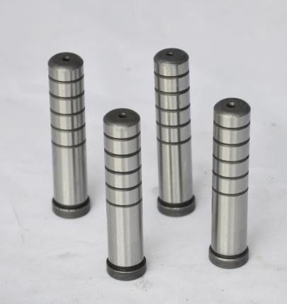
- Machined copper inserts
- Built-in grounding channels routed into mold core/cavities
- Raised shielding baffles inside hot runner zones where heat builds fast
- Taped conductive linings in ejector pin bores where static accumulates over cycles
The Key Take-Away Here
I think most readers aren't molders at factories but maybe engineers trying understand whether they need EM-safe tooling, designers aiming to future proof mold designs for Industry 4.0 integration etc… So let me put the key takeaways upfront before proceeding into examples below.
What You Should Know Before Trying Copper for Shielding Inside Injection Tool Bases:
Copper’s effectiveness depends on geometry: Thickness and shape play a big part. Thin foil vs multi-coat mesh matters!
Don't assume all metal works same in every range Some materials absorb certain spectrum wavelengths better (aluminum = lighter alternative for non-ferrous environments).
Now Back To The Fun Examples...
So if I were prototyping something small, like say testing copper plating over internal surfaces for an RFID-embedded sensor molded inside polypro housing — I’d likely run simulations first with varying metal layer compositions and placement angles against potential wave entry points before cutting anything physical. Because without simulation you'd just be hoping magic metal tape will do miracles later after everything's pressed, hardened… sealed up tight. That’s the danger of trial without modeling first. I've made the error twice – expensive errors both times! First, the mold base failed thermal transfer calibration after applying conductive epoxy strips which messed the flow pattern, and the part deformed. The second try had insufficient shielding coverage and I lost readings half-way though the batch. Lesson? Think through every layer and how its going impact your environment.Mine Craft & My Misplaced Copper Obsession (Kinda)
Ok yes, Minecraft lovers are gonna roll their eyes when mentioning any random keyword combo involving “cooper" or metal crafting. But hey guess what helped spark this obsession further into metallurgical curiosity beyond basic gaming mechanics? Yes indeed! In-game resource management teaches kids about finite material availability long before many realize what the implications truly mean outside of pixels and chests. I learned early how precious ores were… even fake ones simulated via game logic. It wasn’t until playing survival with low spawn rates for copper veins when I became curious about real properties of the thing. Turns out I didn't lose that connection. Now instead of mining for inventory purposes in pixel land... my obsession moved into finding ways copper gets creatively repurposed within technical engineering niches. Whether that means building Faraday cages from recycled scraps OR integrating trace layers into modular assembly stations inside automated manufacturing floors… You see? Games can lead you down interesting professional rabbit holes. Who would’ve thought?Last Section: Practical Advice For Those Curious About Shield Integration Into Mold-Based Setups
So if you're thinking ahead towards setting up protective barriers for delicate electronics while keeping production consistent... Here's my final bit of experience-backed insights that may spare you costly redesign headaches. List Of Best Practices (My Experience Based Approach)- Create prototype shielding modules that you can swap out quick during early trial shots – helps determine ideal material layout without breaking mold design each round.
- If working near high temp areas of the mold base where cooling lines exist close proximity – test copper alloy options with higher melting tolerance otherwise distortion risks shoot sky high mid-use.
- Sometimes the easiest approach is to separate EM sensitive sections entirely via barrier wall between standard injection zone and active control circuits (this applies best for smart injection cell setups only, however – not cost effective always for small-run producers.)
- Remember – conductivity is great BUT oxidation resistance drops over time – especially under humidity stress in factory storage areas. Look into coated finishes like tin plated sheets over untreated copper if moisture is known concern within workspace atmosphere..
- And finally… never skip ESD checks during startup maintenance schedules. Even a single static discharge inside cavity space post-shut off sequence may fry entire control module behind front facing mold frame. It's rare occurrence overall yet happens far too frequently during unmonitored operation hours in large-scale plants.
| Consideration Area | Action Steps | Estimated Cost Increase Factor Over Basic Mold |
| Copper Shield Thickness Adjustment per Frequency Needs | Select based on target application band (LF/HF/etc) | +8% to 15% |
| Incorporate Prebuilt Ground Plane Circuits Along Mold Core Perimeter Areas | Rework waterline paths to include dual purpose channel routing | +22%-30% |
| Mechanical Isolation for Sensors Within Mold Cavity Housing | Add copper foam pads around contact interface points | +18% average (depending material supplier costs local availability etc) |
There you have it.